

Published with permission from Flame Boss, a manufacturer of aftermarket meat smoking controllers.
In this case study, we’re gonna walk through some of the dangers of cost reducing your circuit board in terms of electromagnetic compatibility (EMC) performance.
The subject is a 4 layer design that originally passed EMC testing which was then reduced to a 2 layer design and subsequently failed. We’ll go into the main findings of an initial EMC design review I did on the 4 layer design, then go into the changes needed to get the 2 layer board to pass.
Here’s what we’re going to cover:
- Key findings of an EMC design review of 4 layer circuit board (Subsequently passed at EMC lab)
- 4 layer to 2 layer cost reduction and resulting EMC failure
- Strategy I use to identify and remotely troubleshoot an emissions problem
- Key findings of second EMC design review of 2 layers PCB
- Guidelines: How to optimize 2 layer designs for low emissions performance
Flame Boss Wi-Fi BBQ Smoker

Last year, Roger Collins, owner of Flame Boss, asked me to do an EMC design review of his neat temperature controller device before sending it off to the test house.
The product connects to a smoker or BBQ to monitor the air and meat temperature and a blower accurately controls the temperature profile.
It replaces the mundane task of babysitting the smoker for hours to make sure you get juicy meat. It even has built in Wi-Fi so you can monitor things from a far.
Original EMC design review description and findings
Although the internals to this device weren’t especially high speed (as we’ll get into below), there was still plenty of opportunity for a conducted or radiated emissions failure at a test lab.
I’ve seen simple 25 MHz products fail radiated emissions testing no problem. As we’ll see below, it becomes much more difficult to pass testing when you’re constrained to working on 2 layers.
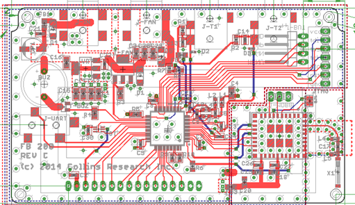
Original 4 Layer PCB
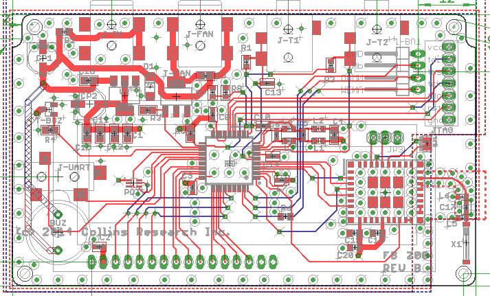
Original 4 Layer PCB Layout
This screenshot shows the original 4 layer PCB layout. The main IC is an NXP MK12DX family (ARM core) MCU running at the default frequency of 20.48 MHz. Not super fast, but not super slow either. It’s the slew (edge) rate anyway that’s more important.
The product has 4 ports that connect to external cabling:
- Port J-IN: 12V DC input (in the top left)
- Port J-FAN: Fan motor PWM drive signals
- Port J-T1/T2: Temperature sensors for air/meat
And 2 connectors for internal connections:
- J_LCD: 8 bit LCD interface
- J-BUT: Button inputs from keypad
In terms of radiated emissions, I was more concerned about the ports that connected to external cabling. At the clock speeds involved in this design, the more likely radiated emissions failure modes are due to common mode currents finding their way out onto external cables.
EMC Standards for the Product
The product was destined for sale to end customers who would probably use it in a residential environment. That meant it would be subject to the more strict ‘class B’ radiated and conducted emission limits – approx 10dB lower emissions than ‘class A’ allowed below 1 GHz.
This just means it could be a bit more difficult to pass radiated and conducted emissions tests, so we’d better put extra effort into EMC design best practices.
Original EMC Design Review Observations & Findings
Given that this design was relatively non-space constrained and there were 4 layers to play with, it wasn’t a big stretch to optimize the design for good emissions performance.
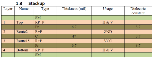
Flame Boss Original 4 Layer PCB Stack
A good place to start with an EMC design review is the foundation of your design – the PCB layer stack. So this is the first place I looked.
In this design, the Flame Boss used the typical PCB stack recommended for 4 layer boards which is routing/components on the top and bottom layers, with the middle two layers reserved for power and ground flood.
As you can see from the thickness dimensions in the table above, the routing layers were tightly coupled together, with a thick core (47 mils) between the GND and VCC layers.
From an EMC perspective, ideally the PWR/GND layers are tightly coupled which increases interplane capacitance. That increases the plane’s ability to provide current at very high frequencies to satisfy any IC’s demand.
But on a 4 layer board, it’s usually preferable to sacrifice the increased interplane capacitance to minimize return path loop areas and make controlled impedance track widths thinner instead.
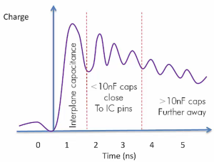
Source of Charge on IC Power Pin With Momentary Current Demand [Source: EMC for PCB Designers (K. Armstrong)]
So, the stack looks good.
6 Objectives for a Good PCB Stack
If you want to evaluate your own PCB stack from an EMC perspective, these are the 6 things you’d ideally like to have. [Source: EMC Compatibility Engineering, Ott].
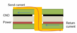
1. Signal layers adjacent to plane
We want the signal (routing) layers to always be adjacent to at least one plane (PWR or GND). That does at least 2 things for us electromagnetically speaking:
(a) It allows us to accurately control the impedance, which if tuned properly, minimizes reflections and optimizes signal integrity and
(b) It means that the return current is at close as physically possible to the send current. That minimizes the differential current loop area and therefore minimizes radiated emissions due to DM current.
For a free tool to calculate signal impedance (and a whole lot of other parameters) check out the awesome PCB toolkit from Saturn PCB.
2. Signal layers tightly coupled to plane
Ideally the signal layers are also tightly coupled to the adjacent plane (as opposed to loosely coupled). This helps with a few things:
- Minimizes current loop area consisting of send and receive paths because the return path is physically close
- As the trace and the plane move closer together, the ground plane inductance decreases (decreasing voltage drop in a plane for a given current
These factors in most cases lead to a reduction in radiated emissions and crosstalk between adjacent traces.
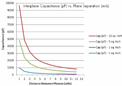
3. PWR + GND planes closely coupled (increased interplane capacitance)
We want power and ground layers to be adjacent and very close to each other. As I mentioned above, this increases interplane capacitance, which allows for more energy storage. Since planes have the lowest inductance of any energy source on your board in the power distribution network, they are the first and best source of energy for instantaneous current demand from IC power pins.
4. High speed signals on buried layers (to contain E-fields + shield critical signals)
We ideally want high speed signals, or more specifically signals with a fast slew rate to be sandwiched between two planes, which helps to contain the E-fields and reduces crosstalk.
5. Multiple GND planes (to decrease return path inductance)
Lastly, we ideally want more than one ground plane. As long as the planes are very well bonded together with stitching vias, this is going to help to lower the ground plane inductance. This will help to keep noise on the ground planes lower (lower voltage noise will be developed for a given amount of noise current). This means less noise is driven onto external cabling which we know is a major potential source of EMI.
6. Critical signals routed on max of 2 layers and referenced to same plane
 If you need to route critical signals on more than one layer, you should use a maximum of two layers and they should be referenced to the same plane. The reason for this is to ensure that the current return path loop area is minimized. If the signal is not referenced to the same plane (like in the example shown on the right here), the return current has to find a way to get from one plane to the other (in this case, the underside of the power plane to the top side of the GND plane).
If you don’t provide a nearby route for that return current, such as a decoupling capacitor located right next to the signal via, then you risk creating a large current loop. Large current loops = potentially good antennas, so we want to avoid that scenario.
Compromise and Prioritization
If you can meet some or most of those objectives, you’re going to be doing better than a lot of hardware manufacturers out there. Seriously, over the years of doing EMC design reviews, I’ve come across lots of boards where the designer has not even specified layer thicknesses and in some cases also didn’t specify layer order. So essentially they would be working with unknown impedances on their board meaning signal integrity is unknown.
It’s impossible to satisfy all 6 of these criteria with any less than an 8 layer board, so for a 4 layer board like this, we need to make some educated trade offs.
If you’re looking for some guidance here, I would suggest that the first two objectives are the most important, so I’d always recommend implementing these two.
These objectives also mean that it’s important to have a dialog going with your PCB manufacturer to make sure that they can accommodate the stack geometries that you want. There’s usually a bit of back and forth with the manufacturer to see what their standard pre-preg and core thicknesses are, then you can go off and calculate your track and gap dimensions based on that information to achieve the impedances that you want.
List of EMC/EMI Improvement Recommendations
Back to the 4 layer EMC design review.
Although the design possibly would have passed emissions testing without any changes, the EMC design review was an opportunity to improve the electromagnetic performance and de-risk the certification process.
The main items I recommended changing in the original 4 layer design were:
- Improve decoupling in several specific areas
- Optimize decoupling by improving decoupling cap orientation and via spacing
- Increase track width of several power supply rails to decrease PDN impedance (and reduce power supply noise)
- Add ferrites for local analog supply rails and RF supply rail
- Re-routed some parts of the circuit board to minimize tracks on the back of the PCB
- Pin swap LCD interface on MCU to make signals flow to connector without jumping layers
- Insert series resistors on several serial interface signals to add some slew rate limiting and termination. Or at least place 0 ohm placeholders to use as get out of jail free cards
- Insert placeholders for R-C low pass filters on each signal heading off to LCD
- Reduce drive strength on all driven signals from MCU where bandwidth allows
- Add GND stitching vias across the board every 10mm-20mm to reduce possibility of plane resonance happening
- Use shielded cable for PWM fan
- Recommend adding ESD protection diodes to temperature probe signals as close to connectors as possible
- Add low pass filters (simple R-C) with low bandwidth (e.g. 500 Hz) to analog inputs. This protects against radiated fields coupled to the cabling from radiated immunity EMC testing (61000-4-3).
- Several other items I won’t go into here to mitigate against some other EMC immunity tests.
Updated 4 Layer Design
Based on the initial review, Roger modified the PCB to improve the EMC/EMI performance prior to the final test schedule.
Updated 4 Layer PCB Layout
The GND and PWR plane layers allows us to route signals perpendicular to each other on the top and bottom layers without having to worry too much about cutting the return current paths.
The Initial Radiated Emissions “PASS” Data
According to the test data from the EMC lab, the worst case emission was 14.4 dB under the limit (at 30 MHz). That’s lots of margin, so it’s a very solid pass.
4 to 2 Layer Cost Reduction
A few months later, Roger decided to cost reduce the circuit board and one of the main areas to save money was on the bare board itself.
Depending on order quantities, this could represent 50c – $2 saving per unit [based on a quick online quote], which adds up quickly for high volume consumer devices.
Here’s the new board condensed down to 2 layers.
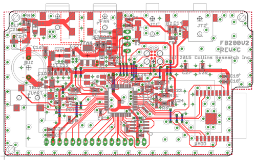
Reduced to 2 Layer PCB
What we can see is that since the internal layers have disappeared, we lose a lot of routing options. As a result, you can see a lot more tracks routed on the bottom side of the PCB, including power and data tracks. This has the significant downside of turning the ground plane (and other return paths) into swiss cheese.
Things suddenly looked not quite so nice and from what I saw of the new design I immediately suspected that there were probably some return path issues that had been introduced.
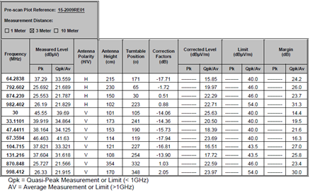
The corresponding emissions scan from the test lab show that some pretty big issues have appeared all the way across the 30 MHz – 500 MHz band.
By the profile of the emissions (frequency, bandwidth, power etc.) it looks like we have 2 or more separate issues to deal with.
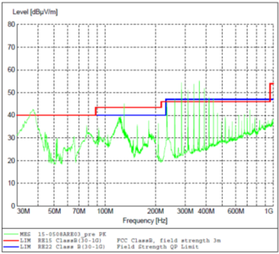
Radiated Emissions Failure
Analyzing the Radiated Emissions Plot
Without having the physical unit available to troubleshoot at my home lab, I needed to make do with making educated guesses at the source of emissions.
At an EMC lab or with troubleshooting/pre-compliance equipment at hand, you could confirm the sources very quickly by enabling/disabling areas of the circuitry, disconnecting cables and/or sniffing around with near field probes.
Fortunately just based on the frequency and profile of the emissions involved, coupled with copies of the PCB layout and schematics, I can hazard a few guesses at the noise sources, coupling mechanisms and antenna structures that are responsible.
Bump at 30-40 MHz
With relatively low frequency, broadband ‘bumps’ like the one you can see between 30-40 MHz, I usually suspect things like motor driver circuits or switching power supply circuitry.
Conversely, very repetitive signals like digital signals and clocks tend to be very narrowband because the frequency, slew rate and duty cycles don’t change much.
We do have a PWM circuit on board to drive the fan motor, so I would suspect something could be wrong in the drive path here.
Broadband noise around 120 MHz
Again I’d be looking for anything electro-mechanical first. I noticed there is also a piezo-electric buzzer in the design, which in theory should have been ‘on’ for test purposes. Test labs always want to measure worst case scenario which means every area of your circuit should be operational.
Again, this may not be the issue, but the broadband nature of the emission made me look carefully at the drive paths for both the motor driver and buzzer circuits. With a near field probe set or small GTEM, you could figure it out pretty quickly, but I didn’t have a board in hand to confirm.
Alternatively these sort of bumps could be other variable frequency sources such as dithered clocks, PWM controlled devices or even modulated intentionally radiating signals. The design only has a 2.4 GHz transmitter so I ruled that out because these bumps were much lower frequency.
Narrowband emissions at 100-200 MHz
Narrowband ‘spikes’ like these in this frequency range are typically harmonics of clock frequencies present somewhere on board the product. It could be a main processor clock, or internal core clock (often PLL’d up to a multiple of an external crystal frequency) or a bus clock (e.g. parallel/serial databus switching frequency).
In this case the spikes are spaced at exactly the frequency of the processor clock, so we suspect that it’s noise from the processor that’s being radiated through some mechanism.
In less common circumstances, narrowband spikes up here could perceivably be very high harmonics from a poorly designed switch mode power supply. But with SMPS frequencies in the KHz/low MHz regions, I’d typically expect noise problems to be down under 50 MHz and usually below 30 MHz in the conducted emissions testing region.
Emissions at 200-500 MHz
The narrow spikes about 26 MHz apart at the higher frequencies also appear to be harmonics from a clock in the unit. This is very likely related to the same processor emissions issue, so I’m quietly confident that if we solve that, these harmonics will also decrease in amplitude.
Overall you can see that the device failed at several frequencies by anywhere between 1 and 7 dB.
2 Layer Modifications
I chatted with Roger and discussed the idea of going back to a 4 layer design because there were no guarantees that I’d be able to improve the 2 layer design enough to pass emissions testing. But he wanted to give it a shot anyway, so we proceeded with improving the 2 layer PCB layout.
Rather than go through the design and create a report for him which is what I normally do for a design review, we decided it would be quicker if I just implemented everything then provide a change list afterwards. This sped up the turnaround to only 1 day.
The result is the board below:
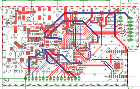
Updated 2 Layer PCB (After EMC Design Review)
What you can notice is that there are way less tracks on the back side of the PCB now. The idea behind this is:
- To minimize ground plane inductance by making the ground plane as big and contiguous as possible
- To minimize the creation of unintentional current loops in the return paths
Here are some of the changes I implemented:
- Added extra decoupling at power supply input
- Re-routed tracks around the RF module to avoid tracks on ground layer as much as possible
- Added decoupling caps at several places along the main power track to maintain low impedance PDN and provide shorter path for noise currents to return to their source
- Moved the big JTAG connector in the upper right hand corner of the PCB closer to MCU to minimize track length and provide more routing space on top layer
- Merged analog/digital grounds and analog/digital power supplies. In this case, separating analog and digital supplies/grounds actually made the performance worse because the extra tracks cause several return path issues
- Prioritized power tracks on the top layer. One of the highest risk areas was the power track routed on the bottom side right across the LCD data signals.
- Moved some components to make the tracks flow more smoothly on the top layer
- Standardized several decoupling capacitor values to 100 nF to avoid creating resonances in the PDN
- Added decoupling next to LCD power pins
- Some other minor tweaks…
Most of the work was moving components and re-routing to avoid tracks on the reverse side of the PCB as much as possible so that the ground plane could remain contiguous and return paths are uninterrupted.
I also improved decoupling in several areas and re-routed the main VCC supply to try to reduce the power supply inductance/impedance.
Although not shown here, I also recommended adding series resistors (0 ohm placeholders or 10-30 ohm-ish) next to the MCU for all drive signals destined to go off board to the LCD. This is like providing yourself with a get out of jail free card if the LCD interface should ever prove to be a problem from a radiated emissions perspective.
Another good contingency is to add X2Y capacitors on the fan motor casing itself and on the PCB next to the motor connector. If there’s any possibility that the fan is causing any component of the noise (e.g. the 30-40 MHz bump or the 120 MHz bump) these X2Y caps can be extremely effective at decoupling the noise currents.
Result
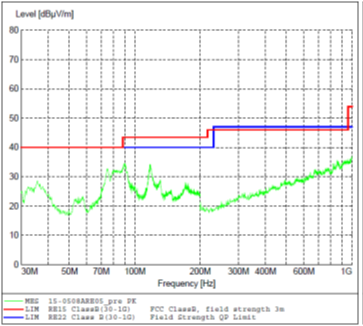
2 Layer Radiated Emissions Pass
After the board was re-manufactured with these changes (and some more that Roger used to finish off the design), the emissions were greatly reduced as you can see above.
The broadband bumps at 30-50 MHz and ~120 MHz were reduced by 5-10 dB.
And the narrowband noise associated with the MCU have disappeared below the noise floor of the analyzer.
Rum and coke’s all around!
Further Resources:
Online training course: EMC Design for Compliance (22 hours)
Recorded webinar: Start to finish EMC design review (2 hours)
eBook: Getting EMC Design Right First Time
Rules of Thumb for 2 Layer Designs
If you’re considering going for a 2 layer board instead of 4, here are a few general guidelines to minimize the risk of having a bad day:
- Assign one full layer to GND if possible.
- Be obsessively compulsive about minimizing components and routing on the GND layer to minimize breaks in the return paths
- Place components and connectors in such a way as to minimize overlapping traces (which reduces the necessity of tracks on the GND layer)
- Use GND flood on the top layer and stitch to GND layer frequently. That way stray currents can ‘jump’ to the top layer rather than create large loops around tracks on GND layer
- Give priority to power rails and route them on one layer as much as possible
- Add de-coupling caps to the power rails at regular intervals to minimize conducted noise current loop areas and maintain low power supply impedance
Conclusion
So as you can see, cost reducing your PCB can lead to some EMC challenges. It’s worth assigning a risk factor to your budget and timelines if you choose to sacrifice some of the objectives that we’ve just talked about. It’s often cheaper for you to address EMI at the PCB level rather than the enclosure level or even worse, have to pay for customer returns if the performance is really bad.

Comments 18
Thanks for the interesting insight. The info on interpreting the failed frequencies is really helpful. Would love to see some more articles on this.
Hi Phillip, thanks, will add your idea to the list!
Very good article, goes from theory to practical application and the thought process involved. Thanks for sharing the knowledge.
Cheers.
Excelent practice example – more, more, more please!! 🙂
For more study is possible schematic?
Author
Sorry no can do (confidential).
For more study is possible schematic?
Sorry no can do (confidential).
Author
Hi Phillip, thanks, will add your idea to the list!
Author
Cheers.
Very good case study. I have been considering converting my 2-layer PCB design (currently a hobby project) to 4 layers so that in the future passing FCC will be much easier. But I really like the lower cost of the 2-layer board. I had already been following the most important of your suggestions here with regard to the 2-layer board and have been further optimizing in my spare time. I think I might be able to stick with 2 layers. My board has only one off-board connection (LCD), but has denser components and routing. I don’t think I can avoid having many signal traces that are 1-2″ long on the bottom GND food.
I currently have GND flood for bottom layer and VCC flood for top, but I like the idea of making GND flood on both sides and stitching. But doing a good job routing VCC on the top layer (not as a flood) will likely be very difficult. I think my main tradeoff is going to be (1) using stitched GND floods on both top and bottom and try to route VCC well on top, versus (2) leaving top as VCC flood but add more decoupling caps throughout the floods and at the locations where signal traces cross breaks in the floods. Any thoughts on this tradeoff?
Thanks!
Great explanation and guided tour! Keep up the good work
Andy ; Good article. One of the most significant changes was to the connectors; especially the JTAG portion. From a birds eye view its easy to see where the routing paths are going. One other way to optimize is to rotate the MCU 45 degrees. A significant change can be just to moving to different case sizes or connector types. This will create extra routing and plane space, given the same board outline. This methodology is actually old and is used very frequently on RF designs, wherein you start with a copper plane and remove areas, rather than adding them (1980’s rubylith PCB design era). The understanding and checking of individual circuit paths and their respective individual return paths (not ground !) is the key ! Regardless whether its Signal Integrity, Power Integrity, or EMC. Thank you for sharing this with us.
Great article! This kind of real world example is very good. The explanation of the analysis methodology and the theoretical-practical perspective is of great value. More of this please!
Oft-forgotten issue, even for low-clock-speed design, is how “sharp” the edges are – i.e. how fast the semiconductor *process* is. Running a high-speed process at slow clock speeds doesn’t reduce the energy in the edges – as we’ve both seen, even 10MHz clocks & drive signals can have artifacts well above 100MHZ to 200MHz. The series resistors, even for on-board signals, are my get-out-of-jail-free card – a slow clock doesn’t “need” the fast edges available from current semiconductor processes.
Pingback: The Roadmap to Low-EMI PCB Design: 9 Essential Steps - EMC FastPass
Congratulations for the successful remote diagnosis. Already without the RF aspect i’m often surprised about the ignorance in PC board design. The default setting seem to be lanes as broad as a hair so 99% of the copper etched away, of course no groundplane…
Then happy bbq. This is the original meaning of bbq, in europe we say bbq when we are actually grilling.