
An EMC FastPass reader reached out to me to share a paper that they had recently written that outlines a solution they found to a radiated emissions problem. They were kind enough to let me reproduce the paper on this blog so that EMC FastPass readers could also benefit from the information. That got me to thinking that other folks probably have a ton of similar stories about failures, troubleshooting and solutions. If you also want to share, I’ve created an easy form to send me the info here. The more you share, the more we’ll all learn, so please do take the time to let us know what you’ve solved in the past.
We’ve all been there – I remember how annoying it was to have a product I’d designed fail radiated emissions testing for the second time. My boss was annoyed and we were getting loads of pressure to fix it so we could ship the product. Sharing will help the whole EMC FastPass community to improve our odds of passing so please do pass on your stories.
Enter [anonymous] EMC FastPass reader (from a very well known company)…..
Background
There are certain products which ask for isolation requirement to be met. To meet this requirement, we usually make use of isolated DC – DC converters which is an easy and compact solution. Usually this leads to severe electromagnetic interference issues which badly impact the certification/qualification of the product. This is due to the in-built transformer in the Isolated DC – DC converter device, which switches at high frequency, in the range of Mega Hertz. Considerable amount of time and money is spent in debugging and resolving these issues. This paper is intended to address these issues with solutions, which will help the designer to take care at the design stage, thereby saving time & money, the important parameters of the project cost.
A set of experiments & analysis were conducted to find the root-cause of the issue. Some of the trials that were experimented to find the root cause is as follows:
1) Disable the Microcontroller
2) Disable the forward DC-DC converter
3) Disable the isolated DC – DC converter and provide external DC supply.
These experiments clearly indicated that the isolated DC – DC converter was causing the radiated emission issue.
The last experiment led to significant result where the emissions were very much below (6 to 10 dBuV) the limit line. Once the source of emission was identified, various fixes were tried to reduce the emission from the product, so as to qualify the certification for the product. These fixes will be explained in detail in the paper with emission graph plots too. As a part of EMI filter circuit, it would be better to have provision for certain ferrite bead and capacitor in the Isolated DC – DC converter circuit on the PCB or the board during the 1st prototype phase. During the test, different values of these components can be tried out and the EMI filtering circuit can be fine tuned to attain best results. This will avoid more revisions of PCB to be built, which in turn reduces the project total cost & increase the product turn over time.
Introduction
The product developed is used as a diagnostic tool in the field of ECU calibration & maintenance. During the Radio Frequency Interference test, there was a failure. Some analysis was done to arrive at the root cause of the issue.
Why is there an isolation requirement for this product?
One of the product requirements, that was mandatory to be met was the isolation between the CAN & USB section. To meet this requirement, an isolated DC – DC converter & isolated CAN transceiver was used. The isolation was provided on the CAN side and not on the USB side.
Basics of Isolated DC – DC converter:
Isolated power supplies generally include either transformers or optical isolators in both the power and the feedback paths. As a result, isolated power supplies are generally more complex in their design than non isolated power supplies. Maxim’s isolated powers ICs accommodate the necessary isolation components, thereby reducing design complexity and cost. Fig 2 shows the block diagram of Isolated DC-DC converter.
Transformer
A key component in any isolated power supply is the power transformer. Critical specifications of the power transformer that have a direct impact on efficiency and reliability are the primary and the secondary winding DC and AC resistances, resulting in operating losses. Another key parameter is leakage inductance. Leakage inductance is a critical parasitic element that must be kept as low as possible to maximize power transfer to the secondary. Low leakage inductance also reduces losses in the primary. As with any other switching power supply, component placement is very important. Because of the primary to secondary isolation, the primary and secondary grounds are separated.
DCR01 family is a series of high-efficiency, input isolated, output-regulated DC/DC converters. In addition to 1W nominal, galvanically -isolated output power capability, this range of DC/DCs offer very low output noise, thermal protection, and high accuracy. The DCR01 family is implemented in standard molded IC packaging, giving standard JEDEC outlines suitable for high- volume assembly.
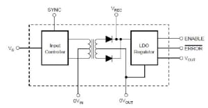
Figure 2: Block Diagram of Isolated DC – DC Converter.
POWER STAGE
The input supply is chopped at a frequency of 400 kHz (internal oscillator divided by 2), which is used to drive the center-tapped toroidal transformer.
RECTIFICATION
The transformer’s output is full wave rectified and smoothed by the external capacitor connected to VREC.
REGULATOR
The internal low drop-out regulator provides a well-regulated output voltage, throughout the operating range of the device.
OSCILLATOR AND WATCHDOG
The DCR01 uses an internal saw-tooth generator to provide the 800 kHz on-board oscillator that is used to drive the power switching circuit. The operation of the oscillator is monitored by the watchdog, which will tri-state the output driver circuit if the oscillator fails, or if the SYNC pin is taken LOW, (shutdown mode). When the SYNC pin is returned HIGH, normal operation resumes. The high switching frequency of 400 kHz allows relatively small values of capacitors to be used for filtering the rectified output voltage. A good quality low ESR capacitor of 1μF placed close to the VREC pin and output ground will reduce the ripple.
CONSTRUCTION
The DCR01 is constructed using a driver IC, low dropout voltage regulator, rectifier diodes, and a wound magnetic toroid, all mounted on a lead frame. The DCR01 requires no special PCB assembly processing, as there is no solder within the package. The result is an isolated DC/DC converter with inherently high reliability.
PCB LAYOUT
The DCR01 is a switching power supply and as such can place high peak current demands on the input supply. In order to avoid the supply falling momentarily during the fast switching pulses, ground and power planes should be used to track the power to the input of DCR01 (this will also serve to reduce noise on the circuit). If this is not possible, the supplies must be connected in a star formation, with the tracks made as wide as possible.
THERMAL MANAGEMENT
Due to the high power density of this device, it is advisable to provide a ground plane on the output. The output regulator is mounted on a copper lead frame within the IC, and a ground plane will serve as an efficient heat sink.
ISSUE DESCRIPTION
This product had to meet radiated emission standard as mentioned below in the table (Table 01). Radiated Emission test was conducted in an anechoic chamber. The distance between the product & the antenna was 10 meters.
Related Post: Emissions Pre-Compliance Testing Guide
Table 01:
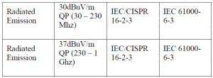
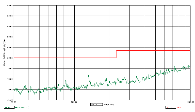
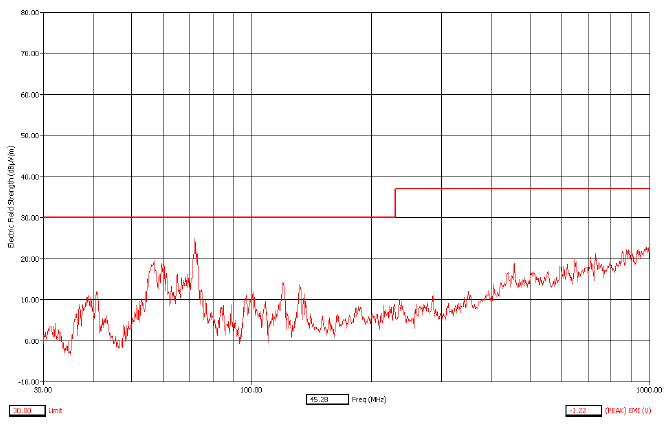
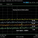
However the test failed at certain frequencies (40 Mhz to 80 Mhz) as the emission crossed the limit of 30dbµV/m at these frequencies. The Radiated Emission plots for both the Horizontal & Vertical is shown in the figure below.
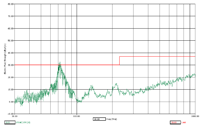
RE Plot: Horizontal: 30MHz to 1GHz
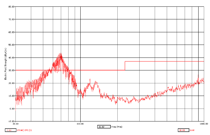
RE Plot: Vertical: 30MHz to 1GHz
The circuit was analyzed carefully. The circuit design for the DCR converter section had a simple capacitor filter at the input & the output stage. The recommended capacitor value was, 1 to 2.2uF & the same was used as shown below in Fig 3. U4 is the reference designator for the DCR converter IC chip. [Note – I’ve quickly manually drawn this schematic. The circuit symbols do not exactly match the actual ICs]
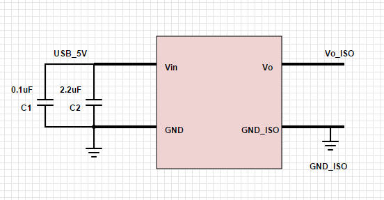
Figure 3: Isolated DC–DC DCR converter circuit with simple Capacitor filter on the Input side.
Analysis done to find the root cause
Many experiments were conducted to find out the root casue for the issue. The following components microcontroller, power supply chips (both isolated & non-isolated) used in the board, were suspected. These were suspected as they were switching at high frequencies. As a part of the analysis, each component was disabled and the radiated Emission test was conducted few times. The plots captured were analyzed further. [Note: this is a very good way to track down the source of radiated emissions. Disable parts of the circuit and disconnect cables until the noise reduces or disappears].
One of the experiments that revealed which component was contributing significantly to radiated emission was “Disabling the Isolated DCR converter”. During this experiment, the DCR converter was disabled. An external linear DC supply was used to power the CAN circuit. Then the radiated emission plot was captured. The plots are shown below for reference. The emissions in these plots were very much below the limit line. This test clearly indicated that the DCR converter caused the radiated emission test failure.
RE Plot: Horizontal, 30 MHz to 1 GHz with DCR converter disabled.
RE Plot: Vertical, 30 MHz to 1 GHz with DCR converter disabled.
Various solutions tried to fix the issue
1) Add Ferrite bead on the Power line on the Input side of the DCR converter:
EMC filter with a ferrite bead on Power line, on the input side of the DCR converter was used. Usually, a single filter on each side of the circuit board will handle the EMC requirements. However this fix did not help much. [Note – I’ve quickly manually drawn this schematic. The circuit symbols do not exactly match the actual ICs]
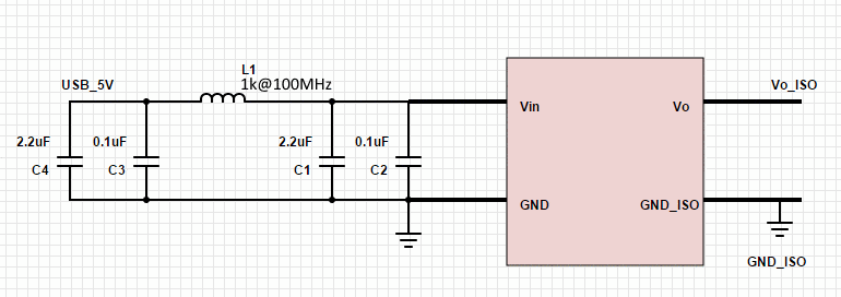
Figure 4: PI-Filter provided on the Input side on the Power Line.
2) Recommended PI filter from Texas Instrument:
To meet international regulations for radio frequency interference (RFI) on equipment and system level there is often a need for some sort of EMC filter on the input & output side of the DC/DC converters. Similar ferrite bead was used on the ground line of the converter.
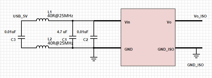
Figure 6: PI-Filter provided on both the Power & Ground Line.
Though there was ferrite bead provided on both the Power & Ground line on the input side of the DCR converter, the issue was not resolved and also did not show any significant improvement in the radiated emission plots.
3) Final Solution which resolved the EMC issue:
In addition to the above ferrite bead solution, high voltage capacitors of few nF/pF (nano Farad/pico Farad) were connected between the input ground & the output ground line of the DCR converter. During this experiment, various values of high voltage capacitors were tried to lower the radiated emission value much below the limit line to have enough margin. The final values of the capacitors 22pF, 0.01uF are shown below in the circuit (mistake in diagram, should show 22pF). The capacitors chosen were rated for high voltage as the design had to meet the Isolation requirement of the product. [Note – I’ve quickly manually drawn this schematic. The circuit symbols do not exactly match the actual ICs]
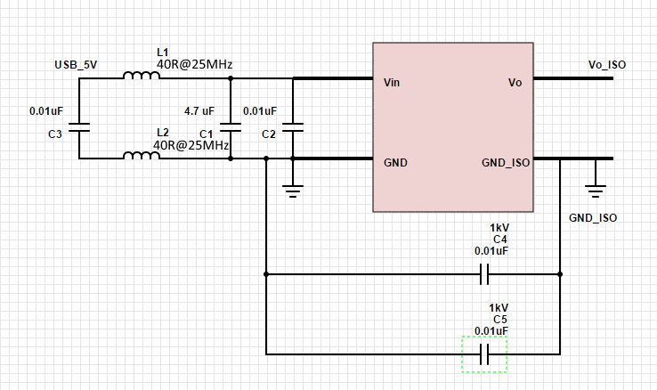
Figure 6: High Voltage capacitors used between the Input ground & Output ground.
Basics of using High voltage capacitors between the two Grounds
Due to high dv/dt (rate of change of voltage) present in switching circuits, currents will flow in any parasitic capacitances. There are parasitic capacitances between transformer primary and secondary. Unless there is a deliberate path for return currents (the completion of the circuit), the parasitic currents will flow in unintended paths. If the unintended paths have a large loop area (as they generally will), the loop will radiate (will cause electromagnetic interference). The capacitor connected between the Input ground & the Output ground, provides a short path, with a small loop area, for parasitic currents. Since it bridges the isolation barrier between primary and secondary, it must be Y2 safety capacitor.
Related Post: How to do an EMC Design Review (see section 3 for more details on bridging slots with capacitors to avoid loop currents)
It’s also worth noting that parasitic currents flowing through resistive and reactive paths can cause potential differences that interfere with sensitive circuits, including, for example, the feedback circuitry of the power supply itself. The capacitance of the bridging cap must be small enough so that leakage currents flowing across the insulation barrier are under a safe limit, typically 0.75mA. This is why the capacitance is usually just a few nF/pF.
SUMMARY/CONCLUSIONS REFERENCES
- Technical datasheet on DCR converter by Texas Instruments: http://www.ti.com/lit/ds/sbvs013c/sbvs013c.pdf
- Technical document: External Synchronization of the DCP01/02, DCR01/02, and DCV01 Series of DC/DC Converters: http://www.ti.com/lit/ds/sbvs013c/sbvs013c.pdf
- DC/DC converters meet most demanding Applications: http://www.irf.com/pressroom/articles/000PE1007.pdf
- Staying Well Grounded by Hank Zumbahlen: http://www.analog.com/library/analogdialogue/archives/46-06/staying_well_grounded.html

Comments 28
Nice post! Thanks to you for sharing !
Author
No problem!
By connecting capacitors between the input and output grounds, isn’t the ground isolation being compromised?
Author
Hi Armando, those caps are rated to 1kV so they’re able to maintain DC isolation up to 1kV. At higher frequencies, the impedance is lower and provides a return path to high frequency currents, which is the whole idea of using them.
Hello.
Every Safety capacitors(Y1, Y2 Capacitor) has isolation voltage level.
Safety caps is disc-type caps and has pin pitch.
Pin pitch must be followed by isolation regulation corresponding application.
(ex. Basic Insulation, 5mm ).
So, Safety caps’ isolation between each other pins are accepted by certification.
So, you can use safety caps between other isolation ground.
Bookmarked, once again 🙂 (bloody switching regulator, I hate you as much as I love you)
Author
Cheers. I hear you!
Thank you so much.
Pingback: Essential EMC Design Rules To Avoid The 7 Most Common EMC Failures - EMC FastPass
One thing to note about adding safety caps: If Hi-Pot testing is required in your device these caps can conduct and cause the test to fail. Ensure you can do a ‘type’ test with the caps removed if doing AC Hi-Pot, or plan to do a DC hi-pot test. I have also found that adding small inductors on both input and output lines can be an effective solution.
OR, do the AC hi-pot with a box that gives total current, reactive current, or real current. Removing parts to do Hi-pot is rather cheating, IMO.
Useful post, if DUT with metallic body shielding would also have better results thou the cap is connected between the terminals
Using a common mode choke could also be a solution. Maybe on both the sides.
Hi
Just wanted to know if the DC to DC Isolated converter 24~12v PCB is enclosed in sheet metal casing, is it a problem, should I use Aluminum Body, or the casing has nothing to do with the test failure
Author
Shielding of DC-DC converter circuitry can definitely help you to pass radiated and conducted emissions testing, but its effectiveness depends on how it is implemented. Too long to go into in the comments section here… I’ll add it to the list of future articles.
Hi Andy,
this is a typical commom mode emission over cable. Instead of Pi-Filter, using common mode choke is more effective and probably cheaper. What do you think?
Author
Hi Tarik, it mentions in the article that they tried CM choke on input power cable and didn’t see much improvement. It’s possible that the choke wasn’t selected with high enough impedance at the noise frequency. Or CM currents could be escaping on other cables. Alternatively a larger choke could be used with 2 or 3 turns of the power wire in there. The other issue is that the magnitude of the DC current can saturate the CM choke, if not size properly, can render the impedance much lower. But the bridging capacitor solution is elegant at minimizing the amount of CM current on external cabling.
Hello ,Andy
Thank you for your nice post with respect to the Radiated Emission(RE) issue,
I’m wondering , is it okay that just putting 1 capacitor here instead of the 2 caps in parallel , because this doubles the probability of failure caused by one of the caps. and the cost is higher.
Hi
Using Y caps, doesnt they increase the leakage currents?
I think reading this article definitely made me realize what’s causing the issue on our isolated DC/DC converter. We have a 470pF capacitor from the input GND to the output GND, but alternatively, we have a 10nF capacitor between the 2 ground planes to help send high voltage, high frequency impulses back to the input earth. This is causing a bigger loop area, and after removing this 10nF capacitor, I can definitely see less noise on my H-field probe. Will be testing this in a TEM cell soon!
Author
Hi Nick, you might also want to check out my new video on DC-DC emissions here: https://www.youtube.com/watch?v=FL0kXwnfV2w
good read, thanks for sharing
hi,
How can we do the measurements using simulation tools ?
I’ve been seeing capacitors between isolated grounds of power supplies but I didn’t know it’s use and thought it defeated the purpose of isolation. You’ve made everything clear to me now. Thank you so much.
Is there a plot available of the emissions spectrum following the bypass capacitor fix? I learned a long time ago that in the certification world, “Because I said so” cuts no ice with the witnesses – everything has to be substantiated by data.
Hi Andy,
Thanks for talking about the return path. But what happens if the isolation is needed over all AC frequencies? We are making power supplies that are attached to the high side of a 600V half bridge, and the 8ns slew rate of the GaN switch means you cannot have any capacitors between input and output as the currents through them become very large. Do you have any suggestions for this situation?
Thanks, Bart
This case study is very useful.
Thanks for sharing. Useful case study